Grypper G35 / G40


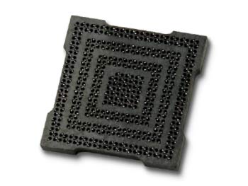
- Package-size PCB footprint: Since the PCB footprint of Grypper is identical to the package, only one PCB design is required, enabling a seamless transition from test and validation through production and reducing overall cost of test
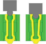
- Low insertion force: Unique contact design reduces the insertion force required to insert and retain higher-ball-count packages safely and securely within the test socket
- Oxide cutting wipe action: The contact design wipes the side of the solder ball during insertion, breaking through solder oxides ensuring a good electrical connection between contact and solder ball
- Signal integrity: A short signal path achieves low inductance and low insertion loss, providing a nearly invisible electrical connection
- Test socket has solder balls attached: The G40 contacts have solder balls reflowed onto the contacts to ensure reliable solder volume at the PCB to test socket solder interface.

Request For Quote or call us at 1-800-404-0204.